1 the introduction
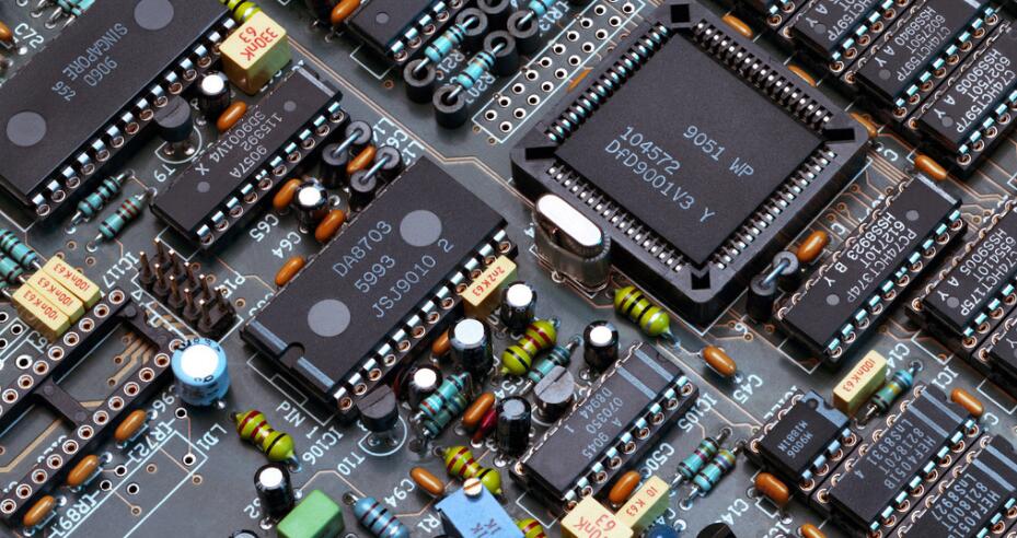
Hybrid Integrated Circuit is an Integrated Circuit which is made of the combination of semiconductor Integrated process and thick (thin) film process.Hybrid integrated circuit (hic) is composed of thick film or thin film components and their interconnection lines made by film-forming method on the substrate, and the mixed assembly of discrete semiconductor chips, monolithic integrated circuits or micro-components on the same substrate, and then the packaging.It has the characteristics of high assembly density, high reliability and good electrical performance.
As the size of the circuit board decreases, the wiring density increases and the working frequency increases, the electromagnetic interference in the circuit becomes more and more prominent.The emc design of circuit board becomes the key of system design.

2.Principle of electromagnetic compatibility
Electromagnetic compatibility (emc) refers to the ability of electronic equipment and power supply to work normally and reliably under certain electromagnetic interference environment.
Any electromagnetic interference must have three basic conditions: the first to have the source of interference, that is, harmful electromagnetic field device or equipment;Secondly, it is necessary to have the way of transmitting interference. Generally, there are two ways: conduction coupling way and radiation coupling way. Thirdly, it is necessary to have sensitive equipment susceptible to interference.Therefore, electromagnetic compatibility problems should be solved one by one according to the three elements of electromagnetic interference.Cutting off the transmission path of interference;Reduce the system's sensitivity to interference.
Electromagnetic interference in hybrid integrated circuit design includes conduction interference, crosstalk interference and radiation interference.When solving the EMI problem, we should first determine whether the coupling path of the emission source is conducted, radiated or crosstalk.If a high transient current or rapidly rising voltage occurs near a conductor carrying a signal, the problem with electromagnetic interference is mainly crosstalk.If there is a complete circuit connection between the source and the sensitive device, the interference is conducted.Radiation interference occurs between two parallel wires that transmit high-frequency signals.
Electromagnetic compatibility design
In the design of electromagnetic compatibility of hybrid integrated circuit, the first thing to do is to do functional inspection. In the circuit determined by the scheme, check whether the electromagnetic compatibility index can meet the requirements. If not, it is necessary to modify the parameters to achieve the index, such as transmission power, working frequency, re-selection of devices, etc.The second is to do protective design, including filtering, shielding, grounding and lap design.The third is to do the layout of the adjustment of the design, including the overall layout of the inspection, components and wire layout inspection.In general, the design of the electromagnetic compatibility of circuits includes: selection of process and components, circuit layout and wiring, etc.
3.1 selection of process and components
There are three manufacturing processes available for hybrid IC: monolayer, multilayer, and multilayer co-firing.Thin film technology can produce small size, low power and high current density components required for high density hybrid circuits, with high quality, stability, reliability and flexibility, suitable for high speed, high frequency and high package density circuits.But can do only one layer wiring and cost is higher.Multi-layer thick film process can produce multi-layer interconnection circuit at a lower cost. From the perspective of electromagnetic compatibility, multi-layer wiring can reduce the electromagnetic radiation of the circuit board and improve the anti-interference ability of the circuit board.Because special power layer and stratum can be set, the distance between signal and ground wire is only the distance between layers.In this way, the loop area of all signals on the board can be minimized, thus effectively reducing the differential mode radiation.
Multilayer co-firing thick film technology has more advantages and is the main technology of passive integration.It can realize more multi-layer wiring, easy to be embedded components, improve assembly density, with good high-frequency characteristics and high-speed transmission characteristics.In addition, it has good compatibility with thin film technology, and the combination of the two can achieve a hybrid multilayer circuit with higher assembly density and better performance.
In the hybrid circuit, the active components usually use the bare chip, and if there is no bare chip, the corresponding encapsulated chip can be used. In order to get the best EMC characteristics, the surface sticker chip should be used as far as possible.The low speed clock should be chosen as far as possible on the premise of satisfying the technical specifications.Never use AC when HC is available, not HC when CMOS4000 is available.Capacitors should have low equivalent series resistance to avoid large attenuation of the signal.
Hybrid circuits can be encapsulated with metal base and shell cover, parallel seam welding, with good shielding effect.
3.2 circuit layout
Three main factors should be considered in the layout division of hybrid microcircuits: the number of input/output pins, device density and power consumption.A useful rule of thumb is that the wafers occupy 20% of the substrate area and dissipate no more than 2W per square inch.
In terms of device layout, in principle, devices related to each other should be placed as close as possible, digital circuit, analog circuit and power circuit should be placed separately, and high-frequency circuit and low-frequency circuit should be separated.Noise - prone devices, low - current circuits, high - current circuits should be kept away from logic circuits.Main interference and radiation sources such as clock circuit and high frequency circuit should be arranged separately away from sensitive circuit.The I /O chip is located near the I /O exit of the hybrid package.
High-frequency components should shorten the connection line as much as possible to reduce the distributed parameters and mutual electromagnetic interference. Vulnerable components should not get too close to each other, and the input and output should be as far away as possible.The oscillator should be as close to the position of the clock chip as possible and away from the signal interface and low level signal chip.The components should be parallel or perpendicular to one side of the substrate, so that the components can be arranged in parallel as far as possible. This will not only reduce the distribution parameters between components, but also conform to the manufacturing process of hybrid circuit, which is easy to produce.
The lead-out pads for power and grounding on the mixed circuit substrate shall be arranged symmetrically, preferably with many power and grounding I/O connections evenly distributed.The mount area of the bare chip is connected to the most negative potential plane.
When choosing multi-layer hybrid circuit, the arrangement between layers of the circuit board changes with the specific circuit, but generally has the following characteristics.
(1) the power supply and the stratum are distributed in the inner layer, which can be regarded as the shielding layer, which can well suppress the inherent common mode RF interference on the circuit board and reduce the distribution impedance of the high-frequency power supply.
(2) the power supply plane and the ground plane in the board should be as close as possible to each other. Generally, the ground plane is above the power supply plane. In this way, interlayer capacitance can be used as the smooth capacitance of the power supply.
(3) the wiring layer should be arranged as close as possible to the power supply or ground plane to generate flux cancellation.
3.3 wire layout
In the circuit design, the focus is often only on improving the wiring density, or the pursuit of uniform layout, ignoring the influence of the circuit layout on the prevention of interference, so that a large number of signals radiate into the space to form interference, which may lead to more electromagnetic compatibility problems.Therefore, good wiring is the key to successful design.
3.3.1 layout of ground wire
Ground wire is not only the potential reference point of the circuit, but also the low impedance circuit of the signal.The common interference on the ground wire is the interference caused by the earth loop current.Solving this kind of interference problem is equal to solving most electromagnetic compatibility problems.The noise on the ground wire mainly affects the ground level of the digital circuit, and the digital circuit is more sensitive to the noise of the ground wire when the output is low.The interference on the ground wire may not only cause the wrong action of the circuit, but also cause conduction and radiation emission.Therefore, the key to reducing these disturbances is to minimize the ground impedance as much as possible (for digital circuits, reducing the ground inductance is particularly important).
The layout of ground wire should pay attention to the following points:
(1) ground wires are set for digital circuit and analog circuit according to different power supply voltages.
(2) make the common ground wire as bold as possible.In the process of multi-layer thick film, the ground wire surface can be specially set, which helps to reduce the area of the loop and also reduces the efficiency of receiving the antenna.And can be used as a signal line shielding.
(3) comb earth wires should be avoided, as they make the signal return loop large, increase radiation and sensitivity, and the common impedance between the chips may cause misoperation of the circuit.
(4) when multiple chips are installed on the board, there will be a large potential difference in the ground wire. The ground wire should be designed as a closed loop to improve the noise tolerance of the circuit.
(5) the circuit board with both analog and digital functions, analog and digital ground is usually separated, only at the power supply connection.
3.3.2 power line layout
In general, except for the interference caused by electromagnetic radiation directly, the electromagnetic interference caused by power line is the most common.Therefore, the layout of the power cord is also important, and the following rules should usually be followed.
(1) the power line should be as close as possible to the ground wire to reduce the area of the power supply loop, and the difference mode radiation is small, which is helpful to reduce the circuit interference.Do not overlap the supply loops of different power sources.
(2) in the multi-layer process, the analog power supply and the digital power supply are separated to avoid mutual interference.Do not overlap the digital power source with the analog power source; otherwise, coupling capacitance will be generated and the separation degree will be destroyed.
(3) the power supply plane and the ground plane can be completely dielectric isolation, frequency and speed is very high, should choose low dielectric paste.The power supply plane should be close to the ground plane and arranged below the ground plane to shield the radiation current distributed in the power supply plane.
(4) the power pin of the chip and the ground lead shall be decoupled.The decoupling capacitor adopts 0.01uF chip capacitor, which should be installed close to the chip to minimize the circuit area of the decoupling capacitor.
(5) when choosing SMD chip, try to choose the chip with power pin and ground pin close to each other, which can further reduce the area of power supply circuit of decoupling capacitor and facilitate the realization of electromagnetic compatibility.
3.3.3 layout of signal lines
In the case of the single-layer film process, a simple and applicable method is to lay out the ground wires first, then to lay out the key signals, such as high-speed clock signals or sensitive circuits near their ground circuits, and finally to lay out other circuits.Signal line layout according to the best signal flow sequence arrangement, so that the circuit board on the signal flow smoothly.
If EMI is to be minimized, the signal line should be as close as possible to the backflow signal line formed by it to minimize the loop area and avoid radiation interference.Low level signal channel should not be close to high level signal channel and power line without filter. Noise-sensitive wiring should not be parallel to high current and high speed switch line.If possible, arrange all key runs in ribbon lines.Incompatible signal lines (digital and analog, high and low speed, high and low current, high and low voltage, etc.) should be kept away from each other. Do not run parallel lines.Crosstalk between signals is extremely sensitive to the length and spacing of adjacent parallel lines, so try to make high-speed signal lines with larger spacing and smaller parallel lengths.
The inductance of the conducting band is proportional to the logarithm of its length and length and inversely proportional to the logarithm of its width.Therefore, the guide tape should be as short as possible, and each address line or data line of the same component should keep the same length as far as possible. As the input and output wires of the circuit, it is best to avoid adjacent parallel wires. It is better to add a ground wire between them, which can effectively suppress crosstalk.The wiring density of low speed signal can be relatively large, and that of high speed signal should be as small as possible.
In the process of multilayer thick film, in addition to observing the rules of single layer wiring, attention should be paid to: try to design a separate ground surface, and arrange the signal layer adjacent to the stratum.When not in use, a ground wire must be placed near the high frequency or sensitive circuit.The signal lines distributed in different layers should be perpendicular to each other so as to reduce the coupling interference of electric field and magnetic field between lines.The signal lines on the same layer should be kept at a certain distance. It is better to isolate the corresponding ground wire circuit to reduce signal crosstalk between lines.Each high - speed signal line should be limited to the same layer.The signal line should not be too close to the edge of the substrate, otherwise it will cause the change of the characteristic impedance, and it is easy to generate the edge field, increasing the outward radiation.
3.3.4 clock circuit layout
Clock circuit plays an important role in digital circuit and is the main source of electromagnetic radiation.A clock signal with a 2ns rising edge radiates energy in a spectrum of up to 160MHz.Therefore, designing a good clock circuit is the key to ensure the electromagnetic compatibility of the whole circuit.Regarding the layout of the clock circuit, there are the following considerations:
(1) do not use Daisy chain structure to transmit the clock signal, but use star structure, that is, all the clock load is directly connected to the clock power driver.
(2) all guide bands connected to the crystal oscillator input/output terminals should be as short as possible to reduce noise interference and influence of distributed capacitance on crystal oscillator.
(3) the crystal capacitor ground wire should be connected to the device with as wide and short guide tape as possible;The nearest digital ground pins to the crystal oscillator should have as few holes as possible.
4 conclusion
In this paper, the causes of electromagnetic interference in hybrid integrated circuits are described in detail, and the problems that should be paid attention to and the specific measures taken in the design of system electromagnetic compatibility are put forward according to the process characteristics of hybrid integrated circuits, which lays a foundation for improving the electromagnetic compatibility of hybrid integrated circuits.

 英语
英语  中文
中文  德语
德语  韩语
韩语  日语
日语  波斯语
波斯语  葡萄牙语
葡萄牙语  俄语
俄语  西班牙语
西班牙语 


